Faraday Electronics FE3030 Data Buffer
The FE3030 is an 84-pin PLCC chip that forms part of the FE3400B chipset. It handles the data buffering between the 80286 processor and the PC/AT expansion bus as well as an 8-bit bus for on-board I/O peripherals (keyboard controller, etc)..
I don't have a datasheet for this component; the partial pinout described below was discovered by probing a GRiDCase 1520 laptop.
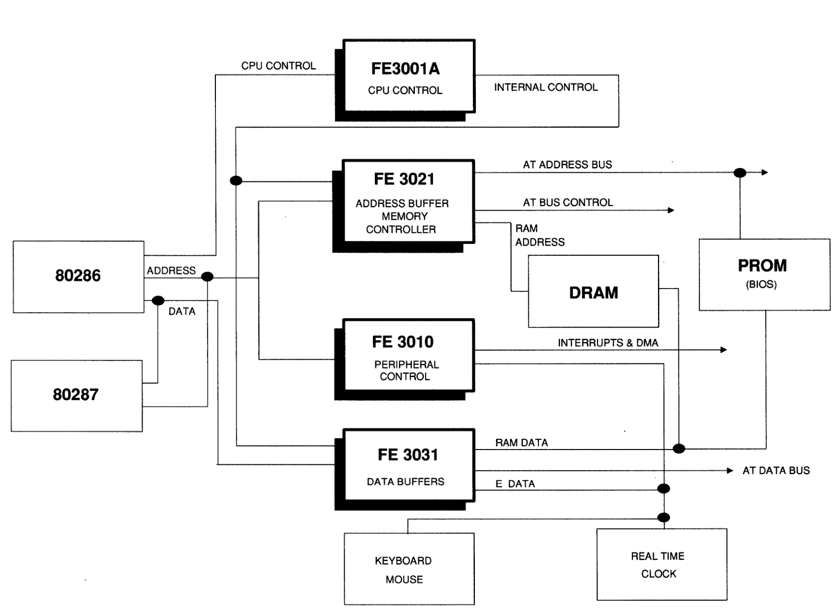
The "FE3001A AT Clock Generation and Cycle Control Device" manual has a block diagram (reproduced below) which references the FE3031 Data Buffer. I'm not sure what differences (if any) there are between the FE3030 and the FE3031.
Pin Assignments
| XD3 | XD2 | XD1 | XD0 | GND | VCC | ED7 | ED6 | ED5 | ED4 | ED3 | ED2 | ED1 | ED0 | GND | ||||||||||
| 11 | 10 | 9 | 8 | 7 | 6 | 5 | 4 | 3 | 2 | 1 | 84 | 83 | 82 | 81 | 80 | 79 | 78 | 77 | 76 | 75 | ||||
| VCC | 12 | FE3030 | 74 | VCC | ||||||||||||||||||||
| GND | 13 | 73 | GND | |||||||||||||||||||||
| XD4 | 14 | 72 | ||||||||||||||||||||||
| XD5 | 15 | 71 | ||||||||||||||||||||||
| XD6 | 16 | 70 | ||||||||||||||||||||||
| XD7 | 17 | 69 | ||||||||||||||||||||||
| VCC | 18 | 68 | HLDA | |||||||||||||||||||||
| GND | 19 | 67 | /MASTER | |||||||||||||||||||||
| XD8 | 20 | 66 | ||||||||||||||||||||||
| XD9 | 21 | 65 | ||||||||||||||||||||||
| XD10 | 22 | 64 | GND | |||||||||||||||||||||
| XD11 | 23 | 63 | ||||||||||||||||||||||
| VCC | 24 | 62 | ||||||||||||||||||||||
| GND | 25 | 61 | ||||||||||||||||||||||
| XD12 | 26 | 60 | ADD0 | |||||||||||||||||||||
| XD13 | 27 | 59 | ||||||||||||||||||||||
| XD14 | 28 | 58 | ||||||||||||||||||||||
| XD15 | 29 | 57 | ||||||||||||||||||||||
| /IOW | 30 | 56 | ||||||||||||||||||||||
| GND | 31 | 55 | GND | |||||||||||||||||||||
| VCC | 32 | 54 | VCC | |||||||||||||||||||||
| 33 | 34 | 35 | 36 | 37 | 38 | 39 | 40 | 41 | 42 | 43 | 44 | 45 | 46 | 47 | 48 | 49 | 50 | 51 | 52 | 53 | ||||
| GND | /IOR | D0 | D1 | D2 | VCC | GND | D3 | D4 | D5 | D6 | D7 | D8 | D9 | D10 | D11 | D12 | D13 | D14 | D15 | |||||
| Pin | Purpose | Direction | Notes |
|---|---|---|---|
| 6, 12, 18, 24, 32, 39, 54, 74 | VCC | Power input | +5V DC |
| 7, 13, 19, 25, 31, 33, 40, 55, 64, 73, 75 | GND | Signal ground | Note that pins 33, 64, and 75 are the only ground pins not paired with a VCC pin; they may be signal pins that are strapped to ground. |
| 8-11, 14-17, 20-23, 26-29 | XD0-15 | Output; likely input on /MASTER cycle | PC/AT expansion bus data. |
| 30 | /IOW | Maybe input from FE3000A? Can also be driven by expansion bus. | Driven low (active) on all I/O write cycles. [TechRef 13-9] |
| 34 | /IOR | Maybe input from FE3000A? Can also be driven by expansion bus. | Driven low (active) on all I/O read cycles. [TechRef 13-10] |
| 36-38, 41-53 | D0-D15 | Input; likely output on /MASTER cycle | CPU data bus. |
| 67 | /MASTER | Input | Used by bus masters to take control of expansion bus. |
| 68 | /HLDA | Input | Hold acknowledge from 80286. |
| 76-83 | ED0-7 | Input/output | 8-bit data bus for onboard peripherals (e.g. keyboard controller). |
Unknown Pins
| Pin | Notes |
|---|---|
| 1 | Connects to FE3000A, pin 3. |
| 4 | Connects to FE3000A, pin 16. |
| 56 | Connects to FE3000A, pin 45. |
| 57 | Connects to FE3000A, pin 82. |
| 58 | Connects to FE3000A, pin 46. |
| 59 | Connects to FE3000A, pin 11. |
| 61 | Connects to FE3010B, pin 58. |
| 62 | Connects to FE3000A, pin 75. |
| 63 | Connects to FE3000A, pin 47. |
| 65 | Connects to FE3000A, pin 55. |
| 69 | Connects to FE3000A, pin 51. |
| 71 | Connects to FE3000A, pin 76. |
| 84 | Connects to FE3000A, pin 3. |
| 2, 3, 5, 35, 60, 66, 70, 72 | Connections unknown. |